Get More Information on Semiconductor Metrology and Inspection Equipment Market - Request Sample Report
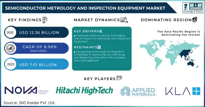
The Semiconductor Metrology and Inspection Equipment Market size was valued at USD 7.01 billion in 2023 and is expected to grow to USD 12.36 billion by 2032 and grow at a CAGR of 6.50 % over the forecast period of 2024-2032.
Semiconductor metrology and inspection are integral to the semiconductor manufacturing process, which involves 400 to 600 steps and takes one to two months to complete. Any flaws detected late in the process can lead to the loss of all efforts in subsequent stages. Effective metrology and inspection are essential for ensuring a high yield and optimal quality. These procedures are implemented at critical stages of production to assess thin films, line widths, pattern defects, and other issues, minimizing costly downtime and maintaining high efficiency. The use of advanced UV light sources in semiconductor inspection is vital for reducing inspection times and improving pattern evaluation accuracy. As the semiconductor industry strives for more compact and high-performance integrated circuits, metrology becomes even more crucial. Companies like TSMC, Infineon, Qualcomm, and Intel are increasing their chip production investments, driving up demand for metrology tools and services. The rise of smartphones, consumer electronics, automotive applications, and IoT devices, particularly with the advent of 5G networks, further fuels the demand for semiconductor materials. The GSMA projects that 5G mobile broadband connections will reach 1.1 billion by 2025, broadening the scope for semiconductor applications across industries. To stay competitive, semiconductor vendors are forming strategic partnerships to develop multifunctional inspection platforms. For example, k-Space Associates introduced the kSA XRF metrology tool, designed to measure thin film thickness with precision. This tool is particularly effective for semiconductor and dielectric layers on substrates like wafers and glass panels. Despite these advancements, the market faces challenges, such as high setup costs, lack of expertise, and geopolitical issues like the US-China trade dispute. These factors hinder the market's growth, although on-demand metrology services are helping mitigate some of these challenges.This evolving market reflects the growing need for semiconductor inspection, metrology systems, 5G technology, and precision measurements to ensure the high quality and efficiency of semiconductor manufacturing processes.
Market Dynamics
Drivers
Advanced Semiconductor Packaging and Its Impact on Metrology and Inspection Equipment
The growing demand for advanced semiconductor packaging methods, such as 3D stacking and system-in-package (SiP) solutions, is driving the expansion of the semiconductor metrology and inspection equipment market. As the industry pushes to develop more compact and powerful devices, advanced packaging techniques play a crucial role in addressing the limits of traditional chip manufacturing. With increasing complexity in designs, particularly in automotive and 5G applications, packaging technologies such as 2.5D and 3D integration are becoming essential to meet the growing demand for smaller, faster, and more efficient semiconductor devices. These advanced packaging methods, which involve stacking multiple dies or chips to increase interconnect density and reduce signal paths, require highly specialized metrology tools. These tools must deliver ultra-precise measurements to detect defects in stacked chips, voids, or delamination at a micrometer level. In sectors like automotive, where semiconductor reliability is crucial for safety, the need for such high-resolution inspection is more important than ever. Advanced packaging offers a solution by combining multiple chips into a single package, thus addressing the limitations of traditional packaging. With applications in AI, IoT, and autonomous vehicles, the need for low-power, high-performance chips is escalating. However, as traditional methods reach their limits, the adoption of advanced packaging is poised to fill the gap. This increased adoption drives the demand for metrology and inspection equipment that can handle these advanced structures with high sensitivity and speed.
Restraints
Navigating Technological Integration Challenges in Semiconductor Metrology and Balancing Innovation with Complex Data Management
A major restraint in the semiconductor metrology and inspection equipment market stems from the challenges associated with integrating a range of advanced metrology tools—optical, X-ray, and electron microscopes—each with distinct calibration and data output requirements. These tools must be synchronized to ensure accurate and consistent defect detection across varying scales, but achieving this integration is complicated by the complexity of aligning different hardware, software, and operator processes. Additionally, the vast amount of data generated by these systems often overwhelms traditional processing pipelines, necessitating advanced, real-time software solutions to effectively manage and analyze the data. Without seamless integration, the risk of delays, errors, and inefficiencies increases, ultimately driving up costs and slowing down market innovation. As semiconductor manufacturing evolves with advanced packaging and smaller structures, the technical barriers to efficient integration hinder the adoption and progress of necessary inspection systems, thereby restraining market growth.
Segment Analysis
by Type
In 2023, the lithography metrology segment dominates the semiconductor metrology and inspection equipment market, of around 41% of total revenue. This leadership is due to its crucial role in supporting advanced manufacturing processes like node miniaturization and producing larger wafer sizes. Lithography metrology tools, such as Critical Dimension Scanning Electron Microscopes (CD-SEMs), ensure the precision and accuracy required for wafer patterning, essential for ultra-large-scale integrated circuits. The segment’s growth is fueled by increasing demand for high-performance semiconductor devices, particularly in AI, 5G, and consumer electronics. Major companies like ASML and KLA continue to lead the segment, pushing advancements in defect detection and mask optimization to strengthen their market position further.
Regional Analysis
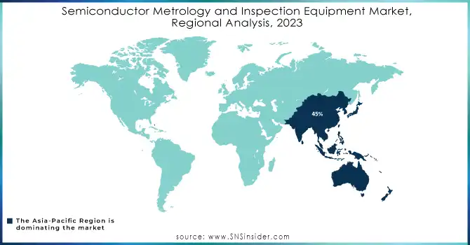
In 2023, the Asia-Pacific region held a dominant share of around 45% in the semiconductor metrology and inspection equipment market, driven by the robust growth of semiconductor manufacturing in Taiwan, South Korea, China, and Japan. Taiwan, with TSMC as a key player, has driven demand for advanced metrology tools due to investments in EUV lithography and 3D packaging. South Korea's semiconductor giants, Samsung and SK Hynix, continue to invest in next-gen technologies like DRAM and NAND flash, fueling the demand for wafer inspection and defect detection. China's push for self-reliance in semiconductor production further accelerates the need for advanced metrology systems. Japan remains a leader in precision equipment, with companies like Tokyo Electron and Nikon at the forefront. The region's continued advancements in AI, 5G, and automotive applications contribute to the strong demand for high-precision inspection systems, ensuring Asia-Pacific remains the largest and fastest-growing market.
In 2023, North America emerged as the fastest-growing region in the semiconductor metrology and inspection equipment market, driven by significant advancements in semiconductor manufacturing and technological innovation. The United States, with key players like Intel, Micron, and GlobalFoundries, has been at the forefront of expanding semiconductor operations. Intel’s investments in next-gen technologies, including advanced process nodes and 3D packaging, have boosted demand for precise metrology tools. Additionally, the U.S. government's CHIPS Act, which supports domestic semiconductor manufacturing, further accelerates growth. Micron’s advancements in memory chips and the rise of AI and 5G technologies also contribute to the region's robust demand for inspection systems. These factors position North America as a leader in semiconductor metrology, sustaining rapid growth.
Need Any Customization Research On Semiconductor Metrology and Inspection Equipment Market - Inquiry Now
Key Players
Some of the major Players in Semiconductor Metrology and Inspection Equipment Market with their product:
KLA Corporation (Advanced process control, metrology, and inspection tools)
Applied Materials, Inc. (Wafer fabrication equipment, metrology, and inspection tools)
Hitachi High-Tech Corporation (SEM-based metrology and inspection solutions)
ASML Holding N.V. (Lithography systems for semiconductor manufacturing)
Nova Measuring Instruments Ltd. (In-line metrology for semiconductor process control)
Nanometrics Incorporated (Wafer metrology and inspection systems)
Rudolph Technologies, Inc. (Metrology systems for semiconductor manufacturing)
Thermo Fisher Scientific Inc. (Scanning electron microscopes, X-ray systems, and metrology tools)
Carl Zeiss AG (Optical and electron microscope systems for semiconductor metrology)
Nikon Corporation (Optical lithography equipment, metrology, and inspection solutions)
Onto Innovation Inc. (Metrology and inspection tools for semiconductor production)
Bruker Corporation (X-ray diffraction, atomic force microscopy, and metrology tools)
Advantest Corporation (Test and inspection equipment for semiconductor devices)
SCREEN Holdings Co., Ltd. (Wafer cleaning and inspection systems)
Camtek Ltd. (Inspection and metrology equipment for semiconductor packaging)
Tokyo Electron Limited (Semiconductor production equipment including metrology tools)
Lam Research Corporation (Metrology and process control tools for semiconductor manufacturing)
ASM International N.V. (Atomic layer deposition, etching, and metrology systems)
Fujifilm Holdings Corporation (Inspection equipment and photomasks for semiconductor manufacturing)
Keysight Technologies, Inc. (Metrology and characterization systems for semiconductor devices)
Qualcomm (Snapdragon SoC processors, 5G modem chips, mobile platform solutions)
TSMC (Taiwan Semiconductor Manufacturing Company) (Advanced semiconductor foundry services, process nodes (7nm, 5nm, 3nm), wafer fabrication)
Infineon Technologies (Power semiconductors, microcontrollers, sensors, automotive chips)
List of Suppliers in Semiconductor Metrology and Inspection Equipment Market:
Raw Material Suppliers for Semiconductor Metrology and Inspection Equipment:
Sumitomo Chemical Co., Ltd.
BASF SE
Air Products and Chemicals, Inc.
Shin-Etsu Chemical Co., Ltd.
Merck Group
Tokyo Ohka Kogyo Co., Ltd. (TOK)
Evonik Industries AG
Cabot Microelectronics Corporation
Dow Inc.
Wacker Chemie AG
Component Suppliers for Semiconductor Metrology and Inspection Equipment:
Coherent, Inc.
Laser Components GmbH
Intel Corporation
STMicroelectronics
Broadcom Inc.
Renesas Electronics Corporation
Teledyne DALSA
Omron Corporation
Keyence Corporation
Photon Systems, Inc.
Recent Development
March 14-Hitachi High-Tech launches the LS9300AD wafer surface inspection system, offering high-sensitivity detection of low-aspect microscopic defects on both front and backside wafer surfaces. Equipped with a new Differential Interference Contrast (DIC) optical system, it improves yield and reduces inspection costs by enabling high-throughput detection of shallow, irregular defects.
Nov 8, 2023, KLA Instruments expands its metrology portfolio with new systems including the Filmetrics® R54-300 for 300mm wafer sheet resistance mapping and the F54-XYT-300 and F60-c film thickness mapping systems, offering enhanced process optimization and automated, high-speed wafer measurement.
November 7, 2024 – Keysight Technologies launched the 4881HV High Voltage Wafer Test System, offering advanced testing capabilities for power semiconductor manufacturers. This system supports testing up to 3kV, streamlines both high- and low-voltage testing in one pass, and integrates with factory automation, enhancing productivity while ensuring compliance with safety regulations.
| Report Attributes | Details |
|---|---|
| Market Size in 2023 | USD 7.01 Billion |
| Market Size by 2032 | USD 12.36 Billion |
| CAGR | CAGR of 6.50 % From 2024 to 2032 |
| Base Year | 2023 |
| Forecast Period | 2024-2032 |
| Historical Data | 2020-2022 |
| Report Scope & Coverage | Market Size, Segments Analysis, Competitive Landscape, Regional Analysis, DROC & SWOT Analysis, Forecast Outlook |
| Key Segments | • By Type (Lithography Metrology, Wafer Inspection, Thin Film Metrology, Other Process Control Systems) |
| Regional Analysis/Coverage | North America (US, Canada, Mexico), Europe (Eastern Europe [Poland, Romania, Hungary, Turkey, Rest of Eastern Europe] Western Europe] Germany, France, UK, Italy, Spain, Netherlands, Switzerland, Austria, Rest of Western Europe]), Asia-Pacific (China, India, Japan, South Korea, Vietnam, Singapore, Australia, Rest of Asia-Pacific), Middle East & Africa (Middle East [UAE, Egypt, Saudi Arabia, Qatar, Rest of Middle East], Africa [Nigeria, South Africa, Rest of Africa], Latin America (Brazil, Argentina, Colombia, Rest of Latin America) |
| Company Profiles | KLA Corporation, Applied Materials, Hitachi High-Tech, ASML Holding, Nova Measuring Instruments, Nanometrics, Rudolph Technologies, Thermo Fisher Scientific, Carl Zeiss, Nikon, Onto Innovation, Bruker Corporation, Advantest, SCREEN Holdings, Camtek, Tokyo Electron, Lam Research, ASM International, Fujifilm Holdings, Keysight Technologies, Qualcomm, TSMC, and Infineon Technologies are major players in the semiconductor industry, offering a wide range of metrology, inspection, and fabrication equipment and services. |
| Key Drivers | • Advanced Semiconductor Packaging and Its Impact on Metrology and Inspection Equipment. |
| RESTRAINTS | • Navigating Technological Integration Challenges in Semiconductor Metrology and Balancing Innovation with Complex Data Management. |
Ans. The Compound Annual Growth rate for Semiconductor Metrology and Inspection Equipment Market over the forecast period is 6.50%.
Ans. The Semiconductor Metrology and Inspection Equipment Market size was valued at USD 7.01 billion in 2023 and is expected to grow to USD 12.36 billion by 2032.
Ans: Asia-Pacific is dominating in Semiconductor Metrology and Inspection Equipment Market in 2023.
Ans: Lithography Metrology is dominating in Semiconductor Metrology and Inspection Equipment Market in 2023.
Ans: KLA Corporation, Applied Materials, Hitachi High-Tech, ASML Holding, Nova Measuring Instruments, Nanometrics, Rudolph Technologies, Thermo Fisher Scientific, Carl Zeiss, Nikon, Onto Innovation, Bruker Corporation, Advantest, SCREEN Holdings, Camtek, Tokyo Electron, Lam Research, ASM International, Fujifilm Holdings, Keysight Technologies, Qualcomm, TSMC, and Infineon Technologies.
Table of Content
1. Introduction
1.1 Market Definition
1.2 Scope (Inclusion and Exclusions)
1.3 Research Assumptions
2. Executive Summary
2.1 Market Overview
2.2 Regional Synopsis
2.3 Competitive Summary
3. Research Methodology
3.1 Top-Down Approach
3.2 Bottom-up Approach
3.3. Data Validation
3.4 Primary Interviews
4. Market Dynamics Impact Analysis
4.1 Market Driving Factors Analysis
4.1.1 Drivers
4.1.2 Restraints
4.1.3 Opportunities
4.1.4 Challenges
4.2 PESTLE Analysis
4.3 Porter’s Five Forces Model
5. Statistical Insights and Trends Reporting
5.1 Wafer Inspection Metrics
5.2 Technology Adoption Rate
5.3 Expenditure on Metrology Equipment
5.4 Backlog of Orders for Semiconductor Equipment
5.5 R&D Investment in Metrology Technologies
6. Competitive Landscape
6.1 List of Major Companies, by Region
6.2 Market Share Analysis, by Region
6.3 Product Benchmarking
6.3.1 Product specifications and features
6.3.2 Pricing
6.4 Strategic Initiatives
6.4.1 Marketing and promotional activities
6.4.2 Distribution and supply chain strategies
6.4.3 Expansion plans and new product launches
6.4.4 Strategic partnerships and collaborations
6.5 Technological Advancements
6.6 Market Positioning and Branding
7. Semiconductor Metrology and Inspection Equipment Market Segmentation, by Application
7.2 Lithography Metrology
7.2.1 Lithography Metrology Market Trends Analysis (2020-2032)
7.2.2 Lithography Metrology Market Size Estimates and Forecasts to 2032 (USD Billion)
7.2.3 Overlay
7.2.3.1 Overlay Market Trends Analysis (2020-2032)
7.2.3.2 Overlay Market Size Estimates and Forecasts to 2032 (USD Billion)
7.2.4 Dimension Equipment
7.2.4.1 Dimension Equipment Market Trends Analysis (2020-2032)
7.2.4.2 Dimension Equipment Market Size Estimates and Forecasts to 2032 (USD Billion)
7.2.5 Mask Inspection and Metrology
7.2.5.1 Mask Inspection and Metrology Market Trends Analysis (2020-2032)
7.2.5.2 Mask Inspection and Metrology Market Size Estimates and Forecasts to 2032 (USD Billion)
7.3 Wafer Inspection
7.3.1 Wafer Inspection Market Trends Analysis (2020-2032)
7.3.2 Wafer Inspection Market Size Estimates and Forecasts to 2032 (USD Billion)
7.4 Thin Film Metrology
7.4.1 Thin Film Metrology Market Trends Analysis (2020-2032)
7.4.2 Thin Film Metrology Market Size Estimates and Forecasts to 2032 (USD Billion)
7.5 Other Process Control Systems
7.5.1 Other Process Control Systems Market Trends Analysis (2020-2032)
7.5.2 Other Process Control Systems Market Size Estimates and Forecasts to 2032 (USD Billion)
8. Regional Analysis
8.1 Chapter Overview
8.2 North America
8.2.1 Trends Analysis
8.2.2 North America Semiconductor Metrology and Inspection Equipment Market Estimates and Forecasts, by Country (2020-2032) (USD Billion)
8.2.3 North America Semiconductor Metrology and Inspection Equipment Market Estimates and Forecasts, by Application (2020-2032) (USD Billion)
8.2.2 USA
8.2.2.1 USA Semiconductor Metrology and Inspection Equipment Market Estimates and Forecasts, by Application (2020-2032) (USD Billion)
8.2.3 Canada
8.2.3.1 Canada Semiconductor Metrology and Inspection Equipment Market Estimates and Forecasts, by Application (2020-2032) (USD Billion)
8.2.4 Mexico
8.2.4.1 Mexico Semiconductor Metrology and Inspection Equipment Market Estimates and Forecasts, by Application (2020-2032) (USD Billion)
8.3 Europe
8.3.1 Eastern Europe
8.3.1.1 Trends Analysis
8.3.1.2 Eastern Europe Semiconductor Metrology and Inspection Equipment Market Estimates and Forecasts, by Country (2020-2032) (USD Billion)
8.3.1.3 Eastern Europe Semiconductor Metrology and Inspection Equipment Market Estimates and Forecasts, by Application (2020-2032) (USD Billion)
8.3.1.4 Poland
8.3.1.4.1 Poland Semiconductor Metrology and Inspection Equipment Market Estimates and Forecasts, by Application (2020-2032) (USD Billion)
8.3.1.5 Romania
8.3.1.5.1 Romania Semiconductor Metrology and Inspection Equipment Market Estimates and Forecasts, by Application (2020-2032) (USD Billion)
8.3.1.6 Hungary
10.3.1.8.1 Hungary Semiconductor Metrology and Inspection Equipment Market Estimates and Forecasts, by Application (2020-2032) (USD Billion)
8.3.1.7 Turkey
8.3.1.7.1 Turkey Semiconductor Metrology and Inspection Equipment Market Estimates and Forecasts, by Application (2020-2032) (USD Billion)
8.3.1.8 Rest of Eastern Europe
8.3.1.8.1 Rest of Eastern Europe Semiconductor Metrology and Inspection Equipment Market Estimates and Forecasts, by Application (2020-2032) (USD Billion)
8.3.2 Western Europe
8.3.2.1 Trends Analysis
8.3.2.2 Western Europe Semiconductor Metrology and Inspection Equipment Market Estimates and Forecasts, by Country (2020-2032) (USD Billion)
8.3.2.3 Western Europe Semiconductor Metrology and Inspection Equipment Market Estimates and Forecasts, by Application (2020-2032) (USD Billion)
8.3.2.4 Germany
8.3.2.4.1 Germany Semiconductor Metrology and Inspection Equipment Market Estimates and Forecasts, by Application (2020-2032) (USD Billion)
8.3.2.5 France
8.3.2.5.1 France Semiconductor Metrology and Inspection Equipment Market Estimates and Forecasts, by Application (2020-2032) (USD Billion)
8.3.2.6 UK
8.3.2.6.1 UK Semiconductor Metrology and Inspection Equipment Market Estimates and Forecasts, by Application (2020-2032) (USD Billion)
8.3.2.7 Italy
8.3.2.7.1 Italy Semiconductor Metrology and Inspection Equipment Market Estimates and Forecasts, by Application (2020-2032) (USD Billion)
8.3.2.8 Spain
8.3.2.8.1 Spain Semiconductor Metrology and Inspection Equipment Market Estimates and Forecasts, by Application (2020-2032) (USD Billion)
8.3.2.9 Netherlands
8.3.2.9.1 Netherlands Semiconductor Metrology and Inspection Equipment Market Estimates and Forecasts, by Application (2020-2032) (USD Billion)
8.3.2.10 Switzerland
8.3.2.10.1 Switzerland Semiconductor Metrology and Inspection Equipment Market Estimates and Forecasts, by Application (2020-2032) (USD Billion)
8.3.2.11 Austria
8.3.2.11.1 Austria Semiconductor Metrology and Inspection Equipment Market Estimates and Forecasts, by Application (2020-2032) (USD Billion)
8.3.2.12 Rest of Western Europe
8.3.2.12.1 Rest of Western Europe Semiconductor Metrology and Inspection Equipment Market Estimates and Forecasts, by Application (2020-2032) (USD Billion)
8.4 Asia-Pacific
8.4.1 Trends Analysis
8.4.2 Asia-Pacific Semiconductor Metrology and Inspection Equipment Market Estimates and Forecasts, by Country (2020-2032) (USD Billion)
8.4.3 Asia-Pacific Semiconductor Metrology and Inspection Equipment Market Estimates and Forecasts, by Application (2020-2032) (USD Billion)
8.4.4 China
8.4.4.1 China Semiconductor Metrology and Inspection Equipment Market Estimates and Forecasts, by Application (2020-2032) (USD Billion)
8.4.5 India
8.4.5.1 India Semiconductor Metrology and Inspection Equipment Market Estimates and Forecasts, by Application (2020-2032) (USD Billion)
8.4.6 Japan
8.4.6.1 Japan Semiconductor Metrology and Inspection Equipment Market Estimates and Forecasts, by Application (2020-2032) (USD Billion)
8.4.7 South Korea
8.4.7.1 South Korea Semiconductor Metrology and Inspection Equipment Market Estimates and Forecasts, by Application (2020-2032) (USD Billion)
8.4.8 Vietnam
8.4.8.1 Vietnam Semiconductor Metrology and Inspection Equipment Market Estimates and Forecasts, by Application (2020-2032) (USD Billion)
8.4.9 Singapore
8.4.9.1 Singapore Semiconductor Metrology and Inspection Equipment Market Estimates and Forecasts, by Application (2020-2032) (USD Billion)
8.4.10 Australia
8.4.10.1 Australia Semiconductor Metrology and Inspection Equipment Market Estimates and Forecasts, by Application (2020-2032) (USD Billion)
8.4.11 Rest of Asia-Pacific
8.4.11.1 Rest of Asia-Pacific Semiconductor Metrology and Inspection Equipment Market Estimates and Forecasts, by Application (2020-2032) (USD Billion)
8.5 Middle East and Africa
8.5.1 Middle East
8.5.1.1 Trends Analysis
8.5.1.2 Middle East Semiconductor Metrology and Inspection Equipment Market Estimates and Forecasts, by Country (2020-2032) (USD Billion)
10.5.1.3 Middle East Semiconductor Metrology and Inspection Equipment Market Estimates and Forecasts, by Application (2020-2032) (USD Billion)
8.5.1.4 UAE
8.5.1.4.1 UAE Semiconductor Metrology and Inspection Equipment Market Estimates and Forecasts, by Application (2020-2032) (USD Billion)
8.5.1.5 Egypt
8.5.1.5.1 Egypt Semiconductor Metrology and Inspection Equipment Market Estimates and Forecasts, by Application (2020-2032) (USD Billion)
8.5.1.6 Saudi Arabia
8.5.1.6.1 Saudi Arabia Semiconductor Metrology and Inspection Equipment Market Estimates and Forecasts, by Application (2020-2032) (USD Billion)
8.5.1.7 Qatar
8.5.1.7.1 Qatar Semiconductor Metrology and Inspection Equipment Market Estimates and Forecasts, by Application (2020-2032) (USD Billion)
8.5.1.8 Rest of Middle East
8.5.1.8.1 Rest of Middle East Semiconductor Metrology and Inspection Equipment Market Estimates and Forecasts, by Application (2020-2032) (USD Billion)
8.5.2 Africa
8.5.2.1 Trends Analysis
8.5.2.2 Africa Semiconductor Metrology and Inspection Equipment Market Estimates and Forecasts, by Country (2020-2032) (USD Billion)
8.5.2.3 Africa Semiconductor Metrology and Inspection Equipment Market Estimates and Forecasts, by Application (2020-2032) (USD Billion)
8.5.2.4 South Africa
8.5.2.4.1 South Africa Semiconductor Metrology and Inspection Equipment Market Estimates and Forecasts, by Application (2020-2032) (USD Billion)
8.5.2.5 Nigeria
8.5.2.5.1 Nigeria Semiconductor Metrology and Inspection Equipment Market Estimates and Forecasts, by Application (2020-2032) (USD Billion)
8.5.2.6 Rest of Africa
8.5.2.6.1 Rest of Africa Semiconductor Metrology and Inspection Equipment Market Estimates and Forecasts, by Application (2020-2032) (USD Billion)
8.6 Latin America
8.6.1 Trends Analysis
8.6.2 Latin America Semiconductor Metrology and Inspection Equipment Market Estimates and Forecasts, by Country (2020-2032) (USD Billion)
8.6.3 Latin America Semiconductor Metrology and Inspection Equipment Market Estimates and Forecasts, by Application (2020-2032) (USD Billion)
8.6.4 Brazil
8.6.4.1 Brazil Semiconductor Metrology and Inspection Equipment Market Estimates and Forecasts, by Application (2020-2032) (USD Billion)
8.6.5 Argentina
8.6.5.1 Argentina Semiconductor Metrology and Inspection Equipment Market Estimates and Forecasts, by Application (2020-2032) (USD Billion)
8.6.6 Colombia
8.6.6.1 Colombia Semiconductor Metrology and Inspection Equipment Market Estimates and Forecasts, by Application (2020-2032) (USD Billion)
8.6.7 Rest of Latin America
8.6.7.1 Rest of Latin America Semiconductor Metrology and Inspection Equipment Market Estimates and Forecasts, by Application (2020-2032) (USD Billion)
9. Company Profiles
9.1 KLA Corporation
9.1.1 Company Overview
9.1.2 Financial
9.1.3 Products/ Services Offered
9.1.4 SWOT Analysis
9.2 Applied Materials, Inc.
9.2.1 Company Overview
9.2.2 Financial
9.2.3 Products/ Services Offered
9.2.4 SWOT Analysis
9.3 Hitachi High-Tech Corporation
9.3.1 Company Overview
9.3.2 Financial
9.3.3 Products/ Services Offered
9.3.4 SWOT Analysis
9.4 ASML Holding N.V.
9.4.1 Company Overview
9.4.2 Financial
9.4.3 Products/ Services Offered
9.4.4 SWOT Analysis
9.5 Nova Measuring Instruments Ltd.
9.5.1 Company Overview
9.5.2 Financial
9.5.3 Products/ Services Offered
9.5.4 SWOT Analysis
9.6 Nanometrics Incorporated
9.6.1 Company Overview
9.6.2 Financial
9.6.3 Products/ Services Offered
9.6.4 SWOT Analysis
9.7 Rudolph Technologies, Inc.
9.7.1 Company Overview
9.7.2 Financial
9.7.3 Products/ Services Offered
9.7.4 SWOT Analysis
9.8 Thermo Fisher Scientific Inc.
9.8.1 Company Overview
9.8.2 Financial
9.8.3 Products/ Services Offered
9.8.4 SWOT Analysis
9.9 Carl Zeiss AG
9.9.1 Company Overview
9.9.2 Financial
9.9.3 Products/ Services Offered
9.9.4 SWOT Analysis
9.10 Nikon Corporation
9.10.1 Company Overview
9.10.2 Financial
9.10.3 Products/ Services Offered
9.10.4 SWOT Analysis
10. Use Cases and Best Practices
11. Conclusion
An accurate research report requires proper strategizing as well as implementation. There are multiple factors involved in the completion of good and accurate research report and selecting the best methodology to compete the research is the toughest part. Since the research reports we provide play a crucial role in any company’s decision-making process, therefore we at SNS Insider always believe that we should choose the best method which gives us results closer to reality. This allows us to reach at a stage wherein we can provide our clients best and accurate investment to output ratio.
Each report that we prepare takes a timeframe of 350-400 business hours for production. Starting from the selection of titles through a couple of in-depth brain storming session to the final QC process before uploading our titles on our website we dedicate around 350 working hours. The titles are selected based on their current market cap and the foreseen CAGR and growth.
The 5 steps process:
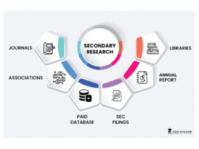
Step 1: Secondary Research:
Secondary Research or Desk Research is as the name suggests is a research process wherein, we collect data through the readily available information. In this process we use various paid and unpaid databases which our team has access to and gather data through the same. This includes examining of listed companies’ annual reports, Journals, SEC filling etc. Apart from this our team has access to various associations across the globe across different industries. Lastly, we have exchange relationships with various university as well as individual libraries.
Step 2: Primary Research
When we talk about primary research, it is a type of study in which the researchers collect relevant data samples directly, rather than relying on previously collected data. This type of research is focused on gaining content specific facts that can be sued to solve specific problems. Since the collected data is fresh and first hand therefore it makes the study more accurate and genuine.
We at SNS Insider have divided Primary Research into 2 parts.
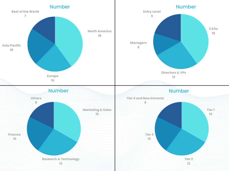
Part 1 wherein we interview the KOLs of major players as well as the upcoming ones across various geographic regions. This allows us to have their view over the market scenario and acts as an important tool to come closer to the accurate market numbers. As many as 45 paid and unpaid primary interviews are taken from both the demand and supply side of the industry to make sure we land at an accurate judgement and analysis of the market.
This step involves the triangulation of data wherein our team analyses the interview transcripts, online survey responses and observation of on filed participants. The below mentioned chart should give a better understanding of the part 1 of the primary interview.
Part 2: In this part of primary research the data collected via secondary research and the part 1 of the primary research is validated with the interviews from individual consultants and subject matter experts.
Consultants are those set of people who have at least 12 years of experience and expertise within the industry whereas Subject Matter Experts are those with at least 15 years of experience behind their back within the same space. The data with the help of two main processes i.e., FGDs (Focused Group Discussions) and IDs (Individual Discussions). This gives us a 3rd party nonbiased primary view of the market scenario making it a more dependable one while collation of the data pointers.
Step 3: Data Bank Validation
Once all the information is collected via primary and secondary sources, we run that information for data validation. At our intelligence centre our research heads track a lot of information related to the market which includes the quarterly reports, the daily stock prices, and other relevant information. Our data bank server gets updated every fortnight and that is how the information which we collected using our primary and secondary information is revalidated in real time.

Step 4: QA/QC Process
After all the data collection and validation our team does a final level of quality check and quality assurance to get rid of any unwanted or undesired mistakes. This might include but not limited to getting rid of the any typos, duplication of numbers or missing of any important information. The people involved in this process include technical content writers, research heads and graphics people. Once this process is completed the title gets uploader on our platform for our clients to read it.
Step 5: Final QC/QA Process:
This is the last process and comes when the client has ordered the study. In this process a final QA/QC is done before the study is emailed to the client. Since we believe in giving our clients a good experience of our research studies, therefore, to make sure that we do not lack at our end in any way humanly possible we do a final round of quality check and then dispatch the study to the client.
Key Segments:
By Type
Lithography Metrology
Overlay
Dimension Equipment
Mask Inspection and Metrology
Wafer Inspection
Thin Film Metrology
Other Process Control Systems
Request for Segment Customization as per your Business Requirement: Segment Customization Request
REGIONAL COVERAGE:
North America
US
Canada
Mexico
Europe
Eastern Europe
Poland
Romania
Hungary
Turkey
Rest of Eastern Europe
Western Europe
Germany
France
UK
Italy
Spain
Netherlands
Switzerland
Austria
Rest of Western Europe
Asia-Pacific
China
India
Japan
South Korea
Vietnam
Singapore
Australia
Rest of Asia Pacific
Middle East & Africa
Middle East
UAE
Egypt
Saudi Arabia
Qatar
Rest of the Middle East
Africa
Nigeria
South Africa
Rest of Africa
Latin America
Brazil
Argentina
Colombia
Rest of Latin America
Request for Country Level Research Report: Country Level Customization Request
Available Customization
With the given market data, SNS Insider offers customization as per the company’s specific needs. The following customization options are available for the report:
Product Analysis
Criss-Cross segment analysis (e.g. Product X Application)
Product Matrix which gives a detailed comparison of the product portfolio of each company
Geographic Analysis
Additional countries in any of the regions
Company Information
Detailed analysis and profiling of additional market players (Up to five)
The Interactive Display Market Size was USD 45.06 billion in 2023 & is expected to reach USD 90.66 billion by 2032 & grow at a CAGR of 8.08% by 2024-2032.
The Rugged Tablet Market Size was valued at USD 0.96 Billion in 2023 and is expected to grow at a CAGR of 6.28% to reach USD 1.66 Billion by 2032.
The RF GaN Semiconductor Device Market size was valued at $1.34 Bn in 2023 and is expected to reach $7.84 Bn by 2032 & grow at a CAGR of 21.7% by 2024-2032
The Milking Robots Market size was valued at USD 2.86 billion in 2023. It is estimated to grow to USD 7.2 billion by 2032 and grow at a CAGR of 10.79% over the forecast period of 2024-2032.
The EMC Filtration Market Size was valued at USD 1.50 Billion in 2023 and is expected to reach USD 2.35 Billion by 2032, at a CAGR of 5.15% During 2024-2032
The Load Break Switch Market Size was valued at USD 3.44 billion in 2023 and is expected to grow at a CAGR of 4.48% to reach USD 5.09 billion by 2032.

Hi! Click one of our member below to chat on Phone
© 2025 All Rights Reserved by SNS Insider Pvt Ltd