The Indium Phosphide Wafer Market size was valued at 179.12 Million in 2024 and is projected to reach USD 472.42 Million by 2032, growing at a CAGR of 12.89% from 2024 to 2032.
Indium Phosphide (InP) Wafer Market growth is strongly due to increasing demand for high-speed, low-energy photonic devices in data centers, artificial intelligence (AI), telecommunications and sensing technologies. The high-frequency low-power optoelectronics such as lasers and photodetectors take the advantage of the superior electron mobility and direct bandgap of InP. The ramp-up of 5G and next-gen data transfer is an important driver for InP.
Coherent’s Texas facility represents an important step in domestic semiconductor growth, fueled by a USD 33 million investment from the U.S. government.
In the United States, the market is also expanding steadily, expected to increase from USD 53.76 Million in 2023 to USD 116.73 million by 2032 at a CAGR of 10.18%. With growing R&D and commercial investments, the global InP wafer market is set for sustained expansion across advanced tech sectors.
In Canada, Université de Sherbrooke developed InP-based solar cells with over 30% efficiency, showcasing national innovation in photonic integration and photovoltaics.
Drivers:
Record-Breaking Solar Cell Efficiency Drives Demand for Indium Phosphide Wafers
As the need for high-efficiency solar cells grows, InP’s unique properties make it ideal for use in next-generation photovoltaic technologies. InP's ability to enable high electron mobility and a direct bandgap position it as a critical material for improving the performance of multi junction solar cells.
For example, just recently, researchers from the Fraunhofer ISE and the AMOLF have reached a record efficiency of 36.1% for a multijunction solar cell based on silicon with GaInP and GaAs. The finding highlights how InP can be used in combination to improve the performance of solar cells, particularly in high-efficiency applications.
Restraints:
Resistance to Transitioning from Silicon to InP-Based Systems
Numerous industries, including telecommunications and data centers, still depend heavily on silicon-based systems. Making the switch to InP-based technology comes with significant expenses on building new infrastructure and retraining employees. Organizations often resist implementing such changes owing to the required high upfront costs and adjustments to existing workflows. This makes companies consider the immediate challenge of pipelines versus the long-term performance and efficiency benefits of switching to InP. Such resistance can hold back the widespread adoption of InP technology even with its benefits.
Opportunities:
Scaling the Future with 6-Inch Indium Phosphide Wafers Unlocking Market Potential
The Indium Phosphide (InP) Wafer Market is entering a transformative phase, with the introduction of the world’s first scalable 6-inch InP wafer manufacturing line by Coherent marking a pivotal shift in production capabilities. As demand surges for AI-driven transceivers, coherent optical communication, and 6G wireless infrastructure, this scale-up in wafer size allows manufacturers to enhance productivity, yield, and performance.
This development increases the number of devices per wafer by a factor of up to four times, resulting in die cost reductions greater than 60%, creating substantial commercial possibilities for next-generation applications including 200G/400G electro absorption modulated lasers (EMLs), high-speed photodetectors and Mach-Zehnder modulators.
Challenges:
Extended R&D Cycles Impacting InP Wafer Technology Adoption
The development and testing of Indium Phosphide (InP)-based devices, such as lasers, photodetectors, and transceivers, require extensive research and development (R&D) efforts. These devices must undergo several stages of development, including design, fabrication, and extensive testing for performance, reliability, and compliance with industry standards. Due to the complex nature of InP wafer technologies and the high precision required in their production, the R&D cycles can be lengthy. This prolonged timeline includes multiple iterations of testing and refinement to ensure the devices meet stringent requirements for high-speed data transmission and low-power consumption. As a result, the adoption of InP wafer technologies in industries like telecommunications, AI, and data centers is slowed down, as businesses are often hesitant to implement new technologies that are still in the lengthy validation phase.
By Diameter
In 2024, the 100 mm (4") segment and higher segment is anticipated to dominate the Indium Phosphide (InP) wafer market, accounting for more than 56% value share of the total industry. The prevalence of High Voltage (HV) and its increased usage for manufacturing high-efficiency optoelectronic devices such as lasers, photodetectors, and transceivers for telecommunication, data centers, and AI infrastructure fueled the largest market size. In addition to accommodating more devices per wafer, larger wafers also increase production efficiency, further driving down per-unit cost and enhancing overall yield.
The 76.2 mm (3") segment of the Indium Phosphide (InP) wafer market is expected to experience the fastest growth from 2025 to 2032. This explosive growth is fueled by demand for small, low-cost wafers that power capabilities across applications we want, such as sensors, high-speed communications, and medical devices. These 3" wafers fill a gap between price and performance in the development of high-end optoelectronic components in support of new technologies such as 5G, automotive connectors, and IoT devices.
By End User
In 2024, the telecommunications segment dominated the Indium Phosphide (InP) wafer market, accounting for approximately 44% of the total revenue. This is driven by the growing need for fast and dependable communication technologies, particularly as 5G networks continue to be rolled out globally and plans for 6G are developed. Indium phosphide (InP) wafers are utilized in the production of optoelectronic elements like lasers, photodetectors, and transceivers that enable sophisticated optical communication systems, which are vital for high-bandwidth data transfer.
The consumer electronics segment is expected to be the fastest-growing sector in the Indium Phosphide (InP) wafer market from 2025 to 2032. The need for low energy consumption, high performance devices is growing with every new mobile devices, electronics and home intelligent systems being introduced into the market, such as smartphones, wearables, smart home products, etc. InP wafers are used to manufacture optoelectronic devices including lasers and photodetectors, which are key technology enablers for advanced sensing, imaging or display technologies in consumer electronics.
In 2024, North America Region is dominated in the Indium Phosphide (InP) wafer market, accounting for around 44% of global revenue, due to the development of an established semiconductor-manufacturing ecosystem, as well as a broad network of research centers, especially in the US. In North America Region the U.S Country dominated the Indium Phosphide Wafer Market. The U.S. benefits from a strong presence of semiconductor fabrication facilities, fostering innovation in InP-based devices for applications like telecommunications, AI, and photonics. The region's ongoing investments in advanced technologies, such as quantum computing and high-performance computing, continue to drive demand for high-quality InP wafers, ensuring North America's prominent position in the global market.
Asia Pacific is projected to be the fastest-growing region in the Indium Phosphide (InP) wafer market during the forecast period with a CAGR 14.66%. The market expansion is due to increasing investments in 5G infrastructure, expansion of the data center network, and growing production house of consumer electronics in China, Vietnam, Japan, South Korea and India. The growing number of telecommunication companies in this region with a well-established supply chain, along with favorable governmental initiatives and the presence of key semiconductor market players adopting Indium Phosphide-based solutions for high-speed data transmission and cutting-edge photonic applications is contributing to the growth of the Indium Phosphide market in this region.
In Asia Pacific Region, the China dominated the Indium Phosphide Wafer Market. The Indium Phosphide (InP) wafer market is dominated by China. China came in first because of its large-scale investments in semiconductors manufacturing, robust government backing with policies such as “Made in China 2025” and fast-growing telecommunications and consumer electronics industries.
Europe maintains a moderate growth position in the Indium Phosphide (InP) Wafer Market, supported by its strong foundation in semiconductor research and advanced technologies. The region shows significant investment in photonics, telecommunications, and data center applications that rely on high-performance InP-based devices. Germany, the UK, and France are leading nations in the development and processing of optoelectronic technologies. With increasing establishment of manufacturing and research facilities, Europe is taking steps to reduce reliance on foreign producers by enhancing its domestic chip-making capabilities. The market is further strengthened by government initiatives aimed at building a resilient and self-sufficient semiconductor ecosystem.
In Latin America and Middle East & Africa Indium Phosphide (InP) wafer market (MEA) is small as compared to the other regions but is likely to experience steady growth, owing to rising investments in telecommunications, data center and emerging technologies. Latin American countries, where demand for InP wafers in optical communications, AI-based applications, is lower than in other regions. The MEA region is also progressively starting to adapt of higher end technologies with nations like UAE and Saudi Arabia aiming for building advanced infrastructure in areas including data center (DC) and optical networks.
Key players in the Indium Phosphide wafer market include Sumitomo Electric Industries, AXT Inc., IntelliEPI Inc., Wafer Technology Ltd., JX Nippon Mining & Metals Corporation, Ortel, Furuya Metal Co., Ltd., MTI Corporation, PAM-XIAMEN, Beijing JiYa Semiconductor Material Co., Ltd.,
On January 2025, Ortel, a subsidiary of Photonics Foundries, transferred its C-Band indium phosphide (InP) laser diode wafer fabrication from Emcore to the Canadian Photonics Fabrication Centre (CPFC) to enhance capacity and ensure supply continuity.
On October 2024, HieFo Corporation announced its participation in the LD Micro Main Event XVII, highlighting its strategic positioning in AI and data center connectivity through high-efficiency indium phosphide (InP) photonic devices. Following its acquisition of EMCORE’s optical core assets, including a world-class North American InP wafer fab, HieFo has solidified its leadership in advanced optoelectronic solutions for next-gen datacom and telecom markets.
| Report Attributes | Details |
|---|---|
| Market Size in 2023 | USD 179.12 Million |
| Market Size by 2032 | USD 472.42 Million |
| CAGR | CAGR of 12.89% From 2024 to 2032 |
| Base Year | 2024 |
| Forecast Period | 2025-2032 |
| Historical Data | 2021-2023 |
| Report Scope & Coverage | Market Size, Segments Analysis, Competitive Landscape, Regional Analysis, DROC & SWOT Analysis, Forecast Outlook |
| Key Segments | • By Diameter (50.8 mm or 2 ", 76.2 mm or 3 ", 100 mm or 4" and Above) • By End User (Consumer Electronics, Telecommunications, Medical, Other End-user Industry Applications) |
| Regional Analysis/Coverage | North America (US, Canada, Mexico), Europe (Eastern Europe [Poland, Romania, Hungary, Turkey, Rest of Eastern Europe] Western Europe] Germany, France, UK, Italy, Spain, Netherlands, Switzerland, Austria, Rest of Western Europe]), Asia-Pacific (China, India, Japan, South Korea, Vietnam, Singapore, Australia, Rest of Asia-Pacific), Middle East & Africa (Middle East [UAE, Egypt, Saudi Arabia, Qatar, Rest of Middle East], Africa [Nigeria, South Africa, Rest of Africa], Latin America (Brazil, Argentina, Colombia, Rest of Latin America) |
| Company Profiles | Key players in the Indium Phosphide wafer market include Sumitomo Electric Industries, AXT Inc., IntelliEPI Inc., Wafer Technology Ltd., JX Nippon Mining & Metals Corporation, Ortel, Furuya Metal Co., Ltd., MTI Corporation, PAM-XIAMEN, Beijing JiYa Semiconductor Material Co., Ltd., and Others |
Ans: The Indium Phosphide Wafer Market is expected to grow at a CAGR of 12.89% during 2025-2032.
Ans: The Indium Phosphide Wafer Market was USD 179.12 Million in 2024 and is expected to Reach USD 472.42 Million by 2032.
Ans: Include the demand for high-speed communication, advancements in semiconductor technology, and the growth of 5G networks.
Ans: The “100 mm or 4" and Above” segment dominated the Indium Phosphide Wafer Market.
Ans: North America dominated the Indium Phosphide Wafer Market in 2024.
Table of Content
1. Introduction
1.1 Market Definition
1.2 Scope (Inclusion and Exclusions)
1.3 Research Assumptions
2. Executive Summary
2.1 Market Overview
2.2 Regional Synopsis
2.3 Competitive Summary
3. Research Methodology
3.1 Top-Down Approach
3.2 Bottom-up Approach
3.3. Data Validation
3.4 Primary Interviews
4. Market Dynamics Impact Analysis
4.1 Market Driving Factors Analysis
4.1.2 Drivers
4.1.2 Restraints
4.1.3 Opportunities
4.1.4 Challenges
4.2 PESTLE Analysis
4.3 Porter’s Five Forces Model
5. Statistical Insights and Trends Reporting
5.1 Wafer Utilization Rate
5.2 Die Per Wafer Ratio
5.3 Energy Consumption per Wafer
5.4 Cycle Time Reduction Trends
6. Competitive Landscape
6.1 List of Major Companies, By Region
6.2 Market Share Analysis, By Region
6.3 Product Benchmarking
6.3.1 Product specifications and features
6.3.2 Pricing
6.4 Strategic Initiatives
6.4.1 Marketing and promotional activities
6.4.2 Distribution and supply chain strategies
6.4.3 Expansion plans and new product launches
6.4.4 Strategic partnerships and collaborations
6.5 Technological Advancements
6.6 Market Positioning and Branding
7. Indium Phosphide Wafer Market Segmentation, by Type
7.1 Chapter Overview
7.2 50.8 mm or 2”
7.2.1 50.8 mm or 2 " Market Trends Analysis (2020-2032)
7.2.2 50.8 mm or 2 " Market Size Estimates and Forecasts to 2032 (USD Million)
7.3 76.2 mm or 3”
7.3.1 76.2 mm or 3 " Market Trends Analysis (2020-2032)
7.3.2 76.2 mm or 3 " Market Size Estimates and Forecasts to 2032 (USD Million)
7.4 100 mm or 4" and Above
7.4.1 100 mm or 4" and Above Market Trends Analysis (2020-2032)
7.4.2 100 mm or 4" and Above Market Size Estimates and Forecasts to 2032 (USD Million)
8. Indium Phosphide Wafer Market Segmentation, by Application
8.1 Chapter Overview
8.2 Consumer Electronics
8.2.1 Consumer Electronics Market Trends Analysis (2020-2032)
8.2.2 Consumer Electronics Market Size Estimates and Forecasts to 2032 (USD Million)
8.3 Telecommunications
8.3.1Telecommunications Market Trends Analysis (2020-2032)
8.3.2 Telecommunications Market Size Estimates and Forecasts to 2032 (USD Million)
8.4 Medical
8.4.1Medical Market Trends Analysis (2020-2032)
8.4.2 Medical Market Size Estimates and Forecasts to 2032 (USD Million)
8.5 Other End-user Industry Applications
8.5.1Other End-user Industry Applications Market Trends Analysis (2020-2032)
8.5.2 Other End-user Industry Applications Market Size Estimates and Forecasts to 2032 (USD Million)
9. Regional Analysis
9.1 Chapter Overview
9.2 North America
9.2.1 Trends Analysis
9.2.2 North America Indium Phosphide Wafer Market Estimates and Forecasts, by Country (2020-2032) (USD Million)
9.2.3 North America Indium Phosphide Wafer Market Estimates and Forecasts, by Type (2020-2032) (USD Million)
9.2.4 North America Indium Phosphide Wafer Market Estimates and Forecasts, by Application (2020-2032) (USD Million)
9.2.5 USA
9.2.5.1 USA Indium Phosphide Wafer Market Estimates and Forecasts, by Type (2020-2032) (USD Million)
9.2.5.2 USA Indium Phosphide Wafer Market Estimates and Forecasts, by Application (2020-2032) (USD Million)
9.2.6 Canada
9.2.6.1 Canada Indium Phosphide Wafer Market Estimates and Forecasts, by Type (2020-2032) (USD Million)
9.2.6.2 Canada Indium Phosphide Wafer Market Estimates and Forecasts, by Application (2020-2032) (USD Million)
9.2.7 Mexico
9.2.7.1 Mexico Indium Phosphide Wafer Market Estimates and Forecasts, by Type (2020-2032) (USD Million)
9.2.7.2 Mexico Indium Phosphide Wafer Market Estimates and Forecasts, by Application (2020-2032) (USD Million)
9.3 Europe
9.3.1 Trends Analysis
9.3.2 Europe Indium Phosphide Wafer Market Estimates and Forecasts, by Country (2020-2032) (USD Million)
9.3.3 Europe Indium Phosphide Wafer Market Estimates and Forecasts, by Type (2020-2032) (USD Million)
9.3.4 Europe Indium Phosphide Wafer Market Estimates and Forecasts, by Application (2020-2032) (USD Million)
9.3.5 Germany
9.3.5.1 Germany Indium Phosphide Wafer Market Estimates and Forecasts, by Type (2020-2032) (USD Million)
9.3.5.2 Germany Indium Phosphide Wafer Market Estimates and Forecasts, by Application (2020-2032) (USD Million)
9.3.6 France
9.3.6.1 France Indium Phosphide Wafer Market Estimates and Forecasts, by Type (2020-2032) (USD Million)
9.3.6.2 France Indium Phosphide Wafer Market Estimates and Forecasts, by Application (2020-2032) (USD Million)
9.3.7 UK
9.3.7.1 UK Indium Phosphide Wafer Market Estimates and Forecasts, by Type (2020-2032) (USD Million)
9.3.7.2 UK Indium Phosphide Wafer Market Estimates and Forecasts, by Application (2020-2032) (USD Million)
9.3.8 Italy
9.3.8.1 Italy Indium Phosphide Wafer Market Estimates and Forecasts, by Type (2020-2032) (USD Million)
9.3.8.2 Italy Indium Phosphide Wafer Market Estimates and Forecasts, by Application (2020-2032) (USD Million)
9.3.9 Spain
9.3.9.1 Spain Indium Phosphide Wafer Market Estimates and Forecasts, by Type (2020-2032) (USD Million)
9.3.9.2 Spain Indium Phosphide Wafer Market Estimates and Forecasts, by Application (2020-2032) (USD Million)
9.3.10 Poland
9.3.10.1 Poland Indium Phosphide Wafer Market Estimates and Forecasts, by Type (2020-2032) (USD Million)
9.3.10.2 Poland Indium Phosphide Wafer Market Estimates and Forecasts, by Application (2020-2032) (USD Million)
9.3.11 Turkey
9.3.11.1 France Indium Phosphide Wafer Market Estimates and Forecasts, by Type (2020-2032) (USD Million)
9.3.11.2 France Indium Phosphide Wafer Market Estimates and Forecasts, by Application (2020-2032) (USD Million)
9.3.12 Rest of Europe
9.3.12.1 UK Indium Phosphide Wafer Market Estimates and Forecasts, by Type (2020-2032) (USD Million)
9.3.12.2 UK Indium Phosphide Wafer Market Estimates and Forecasts, by Application (2020-2032) (USD Million)
9.4 Asia-Pacific
9.4.1 Trends Analysis
9.4.2 Asia-Pacific Indium Phosphide Wafer Market Estimates and Forecasts, by Country (2020-2032) (USD Million)
9.4.3 Asia-Pacific Indium Phosphide Wafer Market Estimates and Forecasts, by Type (2020-2032) (USD Million)
9.4.4 Asia-Pacific Indium Phosphide Wafer Market Estimates and Forecasts, by Application (2020-2032) (USD Million)
9.4.5 China
9.4.5.1 China Indium Phosphide Wafer Market Estimates and Forecasts, by Type (2020-2032) (USD Million)
9.4.5.2 China Indium Phosphide Wafer Market Estimates and Forecasts, by Application (2020-2032) (USD Million)
9.4.6 India
9.4.5.1 India Indium Phosphide Wafer Market Estimates and Forecasts, by Type (2020-2032) (USD Million)
9.4.5.2 India Indium Phosphide Wafer Market Estimates and Forecasts, by Application (2020-2032) (USD Million)
9.4.5 Japan
9.4.5.1 Japan Indium Phosphide Wafer Market Estimates and Forecasts, by Type (2020-2032) (USD Million)
9.4.5.2 Japan Indium Phosphide Wafer Market Estimates and Forecasts, by Application (2020-2032) (USD Million)
9.4.6 South Korea
9.4.6.1 South Korea Indium Phosphide Wafer Market Estimates and Forecasts, by Type (2020-2032) (USD Million)
9.4.6.2 South Korea Indium Phosphide Wafer Market Estimates and Forecasts, by Application (2020-2032) (USD Million)
9.4.7 Singapore
9.4.7.1 Singapore Indium Phosphide Wafer Market Estimates and Forecasts, by Type (2020-2032) (USD Million)
9.4.7.2 Singapore Indium Phosphide Wafer Market Estimates and Forecasts, by Application (2020-2032) (USD Million)
9.4.8 Australia
9.4.8.1 Australia Indium Phosphide Wafer Market Estimates and Forecasts, by Type (2020-2032) (USD Million)
9.4.8.2 Australia Indium Phosphide Wafer Market Estimates and Forecasts, by Application (2020-2032) (USD Million)
9.4.9 Taiwan
9.4.9.1 Taiwan Indium Phosphide Wafer Market Estimates and Forecasts, by Type (2020-2032) (USD Million)
9.4.9.2 Taiwan Indium Phosphide Wafer Market Estimates and Forecasts, by Application (2020-2032) (USD Million)
9.4.10 Rest of Asia-Pacific
9.4.10.1 Rest of Asia-Pacific Indium Phosphide Wafer Market Estimates and Forecasts, by Type (2020-2032) (USD Million)
9.4.10.2 Rest of Asia-Pacific Indium Phosphide Wafer Market Estimates and Forecasts, by Application (2020-2032) (USD Million)
9.5 Middle East and Africa
9.5.1 Trends Analysis
9.5.2 Middle East Indium Phosphide Wafer Market Estimates and Forecasts, by Country (2020-2032) (USD Million)
9.5.3 Middle East Indium Phosphide Wafer Market Estimates and Forecasts, by Type (2020-2032) (USD Million)
9.5.4 Middle East Indium Phosphide Wafer Market Estimates and Forecasts, by Application (2020-2032) (USD Million)
9.5.5 UAE
9.5.5.1 UAE Indium Phosphide Wafer Market Estimates and Forecasts, by Type (2020-2032) (USD Million)
9.5.5.2 UAE Indium Phosphide Wafer Market Estimates and Forecasts, by Application (2020-2032) (USD Million)
9.5.6 Saudi Arabia
9.5.6.1 Saudi Arabia Indium Phosphide Wafer Market Estimates and Forecasts, by Type (2020-2032) (USD Million)
9.5.6.2 Saudi Arabia Indium Phosphide Wafer Market Estimates and Forecasts, by Application (2020-2032) (USD Million)
9.5.7 Qatar
9.5.7.1 Qatar Indium Phosphide Wafer Market Estimates and Forecasts, by Type (2020-2032) (USD Million)
9.5.7.2 Qatar Indium Phosphide Wafer Market Estimates and Forecasts, by Application (2020-2032) (USD Million)
9.5.8 South Africa
9.5.8.1 South Africa Indium Phosphide Wafer Market Estimates and Forecasts, by Type (2020-2032) (USD Million)
9.5.8.2 South Africa Indium Phosphide Wafer Market Estimates and Forecasts, by Application (2020-2032) (USD Million)
9.5.9 Rest of Middle East & Africa
9.5.9.1 Rest of Middle East & Africa Indium Phosphide Wafer Market Estimates and Forecasts, by Type (2020-2032) (USD Million)
9.5.9.2 Rest of Middle East & Africa Indium Phosphide Wafer Market Estimates and Forecasts, by Application (2020-2032) (USD Million)
9.6 Latin America
9.6.1 Trends Analysis
9.6.2 Latin America Indium Phosphide Wafer Market Estimates and Forecasts, by Country (2020-2032) (USD Million)
9.6.3 Latin America Indium Phosphide Wafer Market Estimates and Forecasts, by Type (2020-2032) (USD Million)
9.6.4 Latin America Indium Phosphide Wafer Market Estimates and Forecasts, by Application (2020-2032) (USD Million)
9.6.5 Brazil
9.6.5.1 Brazil Indium Phosphide Wafer Market Estimates and Forecasts, by Type (2020-2032) (USD Million)
9.6.5.2 Brazil Indium Phosphide Wafer Market Estimates and Forecasts, by Application (2020-2032) (USD Million)
9.6.6 Argentina
9.6.6.1 Argentina Indium Phosphide Wafer Market Estimates and Forecasts, by Type (2020-2032) (USD Million)
9.6.6.2 Argentina Indium Phosphide Wafer Market Estimates and Forecasts, by Application (2020-2032) (USD Million)
9.6.7 Rest of Latin America
9.6.7.1 Rest of Latin America Indium Phosphide Wafer Market Estimates and Forecasts, by Type (2020-2032) (USD Million)
9.6.7.2 Rest of Latin America Indium Phosphide Wafer Market Estimates and Forecasts, by Application (2020-2032) (USD Million)
10. Company Profiles
10.1 Sumitomo Electric Industries,
10.1.1 Company Overview
10.1.2 Financial
10.1.3 Products/ Services Offered
10.1.4 SWOT Analysis
10.2 AXT Inc.
10.2.1 Company Overview
10.2.2 Financial
10.2.3 Products/ Services Offered
10.2.4 SWOT Analysis
10.3 IntelliEPI Inc.
10.3.1 Company Overview
10.3.2 Financial
10.3.3 Products/ Services Offered
10.3.4 SWOT Analysis
10.4 Wafer Technology Ltd.
10.4.1 Company Overview
10.4.2 Financial
10.4.3 Products/ Services Offered
10.4.4 SWOT Analysis
10.5 JX Nippon Mining & Metals Corporation
10.5.1 Company Overview
10.5.2 Financial
10.5.3 Products/ Services Offered
10.5.4 SWOT Analysis
10.6 Ortel
10.6.1 Company Overview
10.6.2 Financial
10.6.3 Products/ Services Offered
10.6.4 SWOT Analysis
10.7 Furuya Metal Co., Ltd.
10.7.1 Company Overview
10.7.2 Financial
10.7.3 Products/ Services Offered
10.7.4 SWOT Analysis
10.8 MTI Corporation
10.8.1 Company Overview
10.8.2 Financial
10.8.3 Products/ Services Offered
10.8.4 SWOT Analysis
10.9 PAM-XIAMEN
10.9.1 Company Overview
10.9.2 Financial
10.9.3 Products/ Services Offered
10.9.4 SWOT Analysis
10.10 Beijing JiYa Semiconductor Material Co., Ltd.
10.10.1 Company Overview
10.10.2 Financial
10.10.3 Products/ Services Offered
10.10.4 SWOT Analysis
11. Use Cases and Best Practices
12. Conclusion
An accurate research report requires proper strategizing as well as implementation. There are multiple factors involved in the completion of good and accurate research report and selecting the best methodology to compete the research is the toughest part. Since the research reports we provide play a crucial role in any company’s decision-making process, therefore we at SNS Insider always believe that we should choose the best method which gives us results closer to reality. This allows us to reach at a stage wherein we can provide our clients best and accurate investment to output ratio.
Each report that we prepare takes a timeframe of 350-400 business hours for production. Starting from the selection of titles through a couple of in-depth brain storming session to the final QC process before uploading our titles on our website we dedicate around 350 working hours. The titles are selected based on their current market cap and the foreseen CAGR and growth.
The 5 steps process:
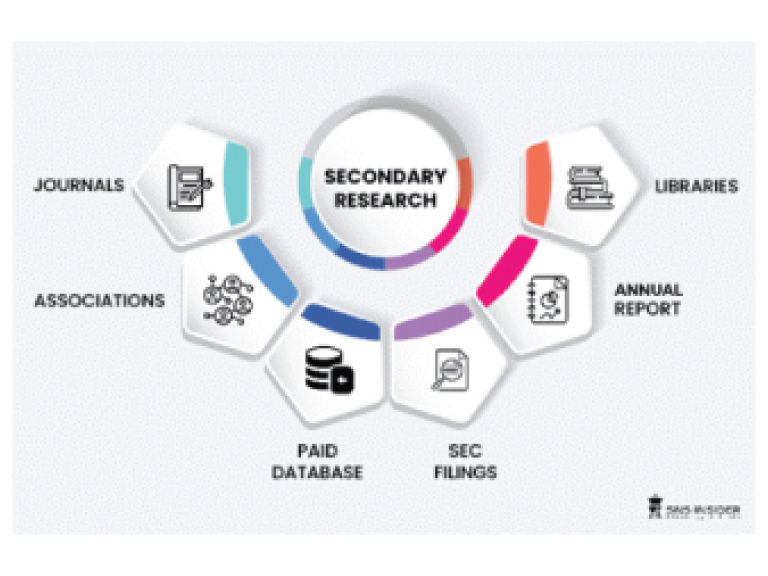
Step 1: Secondary Research:
Secondary Research or Desk Research is as the name suggests is a research process wherein, we collect data through the readily available information. In this process we use various paid and unpaid databases which our team has access to and gather data through the same. This includes examining of listed companies’ annual reports, Journals, SEC filling etc. Apart from this our team has access to various associations across the globe across different industries. Lastly, we have exchange relationships with various university as well as individual libraries.
Step 2: Primary Research
When we talk about primary research, it is a type of study in which the researchers collect relevant data samples directly, rather than relying on previously collected data. This type of research is focused on gaining content specific facts that can be sued to solve specific problems. Since the collected data is fresh and first hand therefore it makes the study more accurate and genuine.
We at SNS Insider have divided Primary Research into 2 parts.
Part 1 wherein we interview the KOLs of major players as well as the upcoming ones across various geographic regions. This allows us to have their view over the market scenario and acts as an important tool to come closer to the accurate market numbers. As many as 45 paid and unpaid primary interviews are taken from both the demand and supply side of the industry to make sure we land at an accurate judgement and analysis of the market.
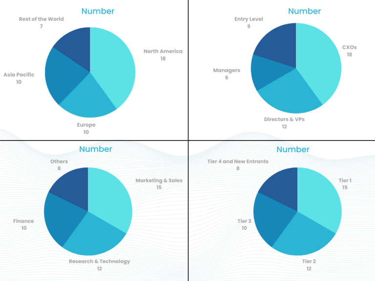
This step involves the triangulation of data wherein our team analyses the interview transcripts, online survey responses and observation of on filed participants. The below mentioned chart should give a better understanding of the part 1 of the primary interview.
Part 2: In this part of primary research the data collected via secondary research and the part 1 of the primary research is validated with the interviews from individual consultants and subject matter experts.
Consultants are those set of people who have at least 12 years of experience and expertise within the industry whereas Subject Matter Experts are those with at least 15 years of experience behind their back within the same space. The data with the help of two main processes i.e., FGDs (Focused Group Discussions) and IDs (Individual Discussions). This gives us a 3rd party nonbiased primary view of the market scenario making it a more dependable one while collation of the data pointers.
Step 3: Data Bank Validation
Once all the information is collected via primary and secondary sources, we run that information for data validation. At our intelligence centre our research heads track a lot of information related to the market which includes the quarterly reports, the daily stock prices, and other relevant information. Our data bank server gets updated every fortnight and that is how the information which we collected using our primary and secondary information is revalidated in real time.

Step 4: QA/QC Process
After all the data collection and validation our team does a final level of quality check and quality assurance to get rid of any unwanted or undesired mistakes. This might include but not limited to getting rid of the any typos, duplication of numbers or missing of any important information. The people involved in this process include technical content writers, research heads and graphics people. Once this process is completed the title gets uploader on our platform for our clients to read it.
Step 5: Final QC/QA Process:
This is the last process and comes when the client has ordered the study. In this process a final QA/QC is done before the study is emailed to the client. Since we believe in giving our clients a good experience of our research studies, therefore, to make sure that we do not lack at our end in any way humanly possible we do a final round of quality check and then dispatch the study to the client.
Key Segments:
By Diameter
50.8 mm or 2 "
76.2 mm or 3 "
100 mm or 4" and Above
By End User
Consumer Electronics
Telecommunications
Medical
Other End-user Industry Applications
Request for Segment Customization as per your Business Requirement: Segment Customization Request
Regional Coverage:
North America
US
Canada
Mexico
Europe
Germany
France
UK
Italy
Spain
Poland
Turkey
Rest of Europe
Asia Pacific
China
India
Japan
South Korea
Singapore
Australia
Taiwan
Rest of Asia Pacific
Middle East & Africa
UAE
Saudi Arabia
Qatar
South Africa
Rest of Middle East & Africa
Latin America
Brazil
Argentina
Rest of Latin America
Request for Country Level Research Report: Country Level Customization Request
Available Customization
With the given market data, SNS Insider offers customization as per the company’s specific needs. The following customization options are available for the report:
Detailed Volume Analysis
Criss-Cross segment analysis (e.g. Product X Application)
Competitive Product Benchmarking
Geographic Analysis
Additional countries in any of the regions
Customized Data Representation
Detailed analysis and profiling of additional market players
The Smart Glass Market Size was valued at USD 6 Billion in 2023 and is expected to reach USD 13.83 Billion by 2032, at a CAGR of 9.76% During 2024-2032
The High Voltage Switchgear Market size was valued at USD 20.53 Billion in 2023. It is estimated to reach USD 30.32 Billion at 4.46% CAGR by 2024-2032
USB Devices Market Size was valued at USD 32.28 billion in 2023 and is expected to reach USD 79.41 billion by 2032 and grow at a CAGR of 10.52 % by 2032.
The Stretchable Conductive Material Market was valued at USD 796.41 million in 2023 and is expected to reach USD 4510.59 million by 2032, growing at a CAGR of 21.28% over the forecast period 2024-2032.
The Programmable Robots Market was valued at USD 3.44 billion in 2023 and is expected to reach USD 13.22 billion by 2032, growing at a CAGR of 16.16% over the forecast period 2024-2032.
The Semiconductor Dry Etch Systems Market was valued at 15.36 billion in 2023 and is projected to reach USD 25.79 billion by 2032, growing at a CAGR of 5.93% from 2024 to 2032.

Hi! Click one of our member below to chat on Phone
© 2025 All Rights Reserved by SNS Insider Pvt Ltd